원본은 NXP 사이트에서 바로 받을 수 있다.
Introduction to Device Trees - 1
Introduction to Device Trees - 2
Introduction to Device Trees - 3
Introduction to Device Trees - 4
Introduction to Device Trees - 5
Introduction to Device Trees - 7
11.1.2 P2020si-pre.dtsi
이 테이블은 p2020si-pre-dtsi 와 e500vs_power_isa.dtsi를 포함하는 Device Tree를 설명한다.
| DTS file | Comments |
|---|---|
| /dts-v1/; | 이 DTS 파일이 DTS version 1을 준수함을 나타냅니다. |
| /include/ “e500v2_power_isa.dtsi” | |
| / { | 루트노드는 forward slash(/)로 구분 |
| compatible = “fsl,P2020”; | 장치 드라이버 선택하는 프로그램에서 사용가능 (예 : 플랫폼별 코드를 선택하는 운영체제) |
| #address-cells = <2>; | 2개의 |
| #size-cells = <2>; | 2개의 |
| interrupt-parent = <&mpic>; | 인터럽트는 MPIC로 연결 |
| aliases { | alias 노드 속성은 다른 노드의 index로 정의 |
| serial0 = &serial0; | |
| serial1 = &serial1; | |
| ethernet0 = &enet0; | |
| ethernet1 = &enet1; | |
| ethernet2 = &enet2; | |
| pci0 = &pci0; | |
| pci1 = &pci1; | |
| pci2 = &pci2; | |
| }; | |
| cpus { | |
| #address-cells = <1>; | 자식노드 reg 속성에서 1개의 |
| #size-cells = <0>; | 자식노드 reg 속성에서 몇 개의 |
| PowerPC,P2020@0 { | PowerPC,P2020 으로 레이블된 노드 |
| device_type = “cpu”; | |
| reg = <0x0>; | CPU 0 |
| next-level-cache = <&L2>; | 다음 레벨 캐시의 포인터 |
| }; | |
| PowerPC,P2020@1 { | |
| device_type = “cpu”; | |
| reg = <0x1>; | CPU 1 |
| next-level-cache = <&L2>; | |
| }; | |
| }; | |
| }; |
11.1.3. P2020si-post.dtsi
post DTSI 파일에는 로컬 버스 및 PCI와 같은 SoC의 주변 장치에 대한 정의가 포함되어 있습니다. 이들 중 다수는 기본 p2020rdb.dts 파일에서 phandles로 참조됩니다. 이 파일에는 특정 주변 장치를 정의하는 다른 많은 DTSI 파일이 포함됩니다. SoC 전용이기 때문에 대부분 이러한 파일을 수정할 필요가 없습니다.
예를 들어, post.dtsi 파일에 아래와 같이 로컬 버스 컨트롤러 정의되어 있다.
&lbc {
	#address-cells = <2>;
	#size-cells = <1>;
	compatible = "fsl,p2020-elbc", "fsl,elbc", "simple-bus";
	interrupts = <19 2 0 0>;
};
이것은 자식 노드가 2개의 주소 셀과 1개의 크기 셀을 갖도록 정의하는 일반적인 노드입니다. LBC 하드웨어는 “fsl, p2020-elbc”, “fsl, elbc”및 “simple-bus”와 호환됩니다. Interrupt는 #19에서 정의되며, 액티브 하이 레벨 감지로 설정됩니다. &lbc는 노드 경로의 레이블입니다.
11.2. LS1021A example
아래는 LS1021A-TWR Device Tree 예제입니다. 이 DTS 파일은 LS1021A-TWR 보드를 설명하고, 그림과 같이 다른 DTSI 파일을 포함합니다.
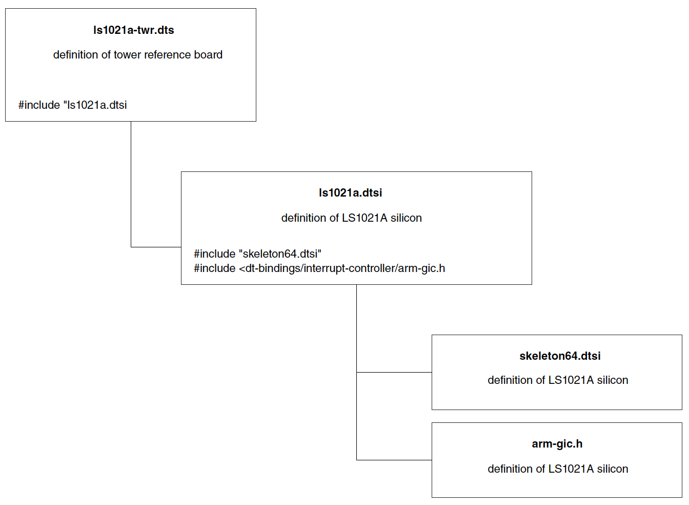
11.2.1. ls1021a-twr.dts
이 테이블은 LS1021A-TWR보를 설명하는 ls1021a-twr.dts 이다.
| DTS file | Comments |
|---|---|
| /dts-v1/; | |
| #include “ls1021a.dtsi” | |
| model = “LS1021A TWR Board”; | device model number |
| aliases { | |
| enet2_rgmii_phy = &rgmii_phy1; | |
| enet0_sgmii_phy = &sgmii_phy2; | |
| enet1_sgmii_phy = &sgmii_phy0; | |
| }; | |
| clocks { | Clocks 노드 |
| sys_mclk: clock { | sys_mclk의 phandle 정의 |
| compatible = “fixed-clock”; | fixed-clock 바인딩을 이용하여 고정 주파수 클럭 정의 |
| #clock-cells = <0>; | Single Clock Output |
| clock-frequency = <24576000>; | Frequency |
| }; | |
| }; | |
| regulators { | |
| compatible = “simple-bus”; | |
| #address-cells = <1>; | |
| #size-cells = <0>; | 자식 노드 셀 중에서 size는 없음 |
| reg_3p3v: regulator@0 { | reg_3p3p phandle, address = 0 |
| compatible = “regulator-fixed”; | |
| reg = <0>; | single address = 0, reg_3p3v: regulator@0 노드의 초기화 주소 |
| regulator-name = “3P3V”; | regulator output name |
| regulator-min-microvolt = <3300000>; | 최소 전압 |
| regulator-max-microvolt = <3300000>; | 최대 전압 |
| regulator-always-on; | regulator는 언제나 enable |
| }; | |
| }; | |
| sound { | |
| compatible = “fsl,vf610-sgtl5000”; | sound에서 쓰이는 특정 드라이버 |
| simple-audio-card,name = “FSL-VF610-TWR-BOARD”; | |
| simple-audio-card,routing = | 오디오 컨포넌트들 사이에 연결은 없다 |
| “MIC_IN”, “Microphone Jack”, | |
| “Microphone Jack”, “Mic Bias”, | |
| “LINE_IN”, “Line In Jack”, | |
| “Headphone Jack”, “HP_OUT”, | |
| “Speaker Ext”, “LINE_OUT”; | |
| simple-audio-card,cpu = <&sai1>; | @sai1 phandle, .dtsi에서 정의 |
| simple-audio-card,codec = <&codec>; | @codec phandle, sgtl5000으로 이후에 정의됨 |
| }; | |
| }; | |
| &dcu0 { | dcu0 phandle |
| display = <&display>; | display phandle |
| status = “okay”; | 디바이스 enable |
| display: display@0 { | display phandle의 주소 0 |
| bits-per-pixel = <24>; | RGB888은 24가 되어야 한다 |
| display-timings { | 자세한 내용은 binding 문서 안에서 display-timing.txt 참조 |
| native-mode = <&timing0>; | |
| timing0: nl4827hc19 { | |
| clock-frequency = <10870000>; | |
| hactive = <480>; | |
| vactive = <272>; | |
| hback-porch = <2>; | |
| hfront-porch = <2>; | |
| vback-porch = <2>; | |
| vfront-porch = <2>; | |
| hsync-len = <41>; | |
| vsync-len = <4>; | |
| hsync-active = <1>; | |
| vsync-active = <1>; | |
| }; | |
| }; | |
| }; | |
| }; | |
| &duart0 { | DTSI 파일에 있는 uart0:label 노드의 확장된 path와 합침 |
| status = “okay”; | ENABLE |
| }; | |
| &duart1 { | uart1:label |
| astatus = “okay”; | |
| }; | |
| &enet0 { | enet0:label |
| tbi-handle = <&tbi1>; | MAC의 TBI interface phandle |
| phy-handle = <&sgmii_phy2>; | 콘트롤러에 연결하는 PHY phandle |
| phy-connection-type = “sgmii”; | 콘트롤러/PHY 인터페이스 = SGMII |
| status = “okay”; | ENABLE |
| }; | |
| &enet1 { | enet1:label |
| tbi-handle = <&tbi1>; | |
| phy-handle = <&sgmii_phy0>; | |
| phy-connection-type = “sgmii”; | |
| status = “okay”; | |
| }; | |
| &enet2 { | enet2:label |
| phy-handle = <&rgmii_phy1>; | |
| phy-connection-type = “rgmii-id”; | 콘트롤러/PHY 인터페이스 = RGMII |
| status = “okay”; | |
| }; | |
| &i2c0 { | i2c0:label |
| status = “okay”; | |
| }; | |
| &i2c1 { | |
| status = “okay”; | |
| codec: sgtl5000@a { | |
| compatible = “fsl,sgtl5000”; | 오디오 드라이버 sgtl5000 사용 |
| reg = <0x0a>; | |
| VDDA-supply = <®_3p3v>; | |
| VDDIO-supply = <®_3p3v>; | |
| clocks = <&sys_mclk 1>; | |
| }; | |
| hdmi: sii9022a@39 { | HDMI phandle, sii9022a 노드의 address = 0x39 |
| compatible = “fsl,sii902x”; | sii902x 드라이버 사용 |
| reg = <0x39>; | 디바이스의 i2c address |
| interrupts = <GIC_SPI 167 IRQ_TYPE_EDGE_RISING>; | interrrupt to the CPU |
| }; | |
| }; | |
| &i2c2 { | i2c2의 노드 패스 레이블 |
| status = “okay”; | |
| monitor: ltc2945@67 { | |
| reg = <0x67>; | |
| }; | |
| }; | |
| &ifc { | ifc:label |
| status = “okay”; | |
| #address-cells = <2>; | |
| #size-cells = <1>; | |
| /* NOR, and CPLD on board */ | ranges 속성은 버스 (자식)의 주소 공간과 부모의 주소 공간 간의 변환매핑. address-cells = 2 이기 때문에 모든 address가 2개의 |
| ranges = <0x0 0x0 0x0 0x60000000 0x08000000 | 자식 노드 address의 0x0 이 부모의 0x6000_0000, size = 0x0800_0000 |
| 0x2 0x0 0x0 0x7fb00000 0x00000100>; | 0x2_0000_0000 -> 0x7fb0_0000 , size = 0x0000_0100 |
| nor@0,0 { | 첫번째 자식 노드, address = 0x0 (부모주소는 0x6000_0000) |
| compatible = “cfi-flash”; | NOR flash 드라이버 |
| #address-cells = <1>; | |
| #size-cells = <1>; | |
| reg = <0x0 0x0 0x8000000>; | 메모리 address = 0x0, size = 0x800_0000 |
| bank-width = <2>; | flash interface width (bytes) |
| device-width = <1>; | single flash device width (bytes) |
| partition@0 { | NOR flash 첫번째 mtd partition |
| /* 128KB for rcw */ | |
| reg = <0x00000000 0x0020000>; | address = 0x0, size = 0x002_0000 |
| label = “NOR bank0 RCW Image”; | MTD 드라이버 레이블 |
| }; | |
| partition@20000 { | NOR flash MTD partition |
| /* 1MB for DTB */ | |
| reg = <0x00020000 0x00100000>; | address = 0x0002_0000(주소는 노드 정의의 주소와 일치), size = 0x0010_0000 |
| label = “NOR DTB Image”; | MTD 드라이버 레이블 |
| }; | |
| partition@120000 { | |
| /* 8 MB for Linux Kernel Image */ | |
| reg = <0x00120000 0x00800000>; | address = 0x0012_0000, size = 0x0080_0000 |
| label = “NOR Linux Kernel Image”; | |
| }; | |
| partition@920000 { | |
| /* 56MB for Ramdisk Root File System */ | |
| reg = <0x00920000 0x03600000>; | address = 0x0092_0000, size = 0x0360_0000 |
| label = “NOR Ramdisk Root File System Image”; | |
| }; | |
| partition@3f80000 { | |
| /* 512KB for bank4 u-boot Image */ | |
| reg = <0x03f80000 0x80000>; | address = 0x03f8_0000, size = 0x8_0000 |
| label = “NOR bank4 u-boot Image”; | |
| }; | |
| partition@4000000 { | |
| /* 128KB for bank4 RCW Image */ | |
| reg = <0x04000000 0x20000>; | address = 0x0400_0000, size = 0x2_0000 |
| label = “NOR bank4 RCW Image”; | |
| }; | |
| partition@4020000 { | |
| /* 63MB JFFS2 ROOT File System Image */ | |
| reg = <0x04020000 0x3f00000>; | address = 0x0402_0000, size = 0x3f0_0000 |
| label = “NOR JFFS2 ROOT File System Image”; | |
| }; | |
| partition@7f80000 { | |
| /* 512KB for bank0 u-boot Image */ | |
| reg = <0x07f80000 0x80000>; | address = 0x07f8_0000, size = 0x8_0000 |
| label = “NOR bank0 u-boot Image”; | |
| }; | |
| }; | |
| }; | |
| &lpuart0 { | lpuart0:label |
| status = “okay”; | |
| }; | |
| &mdio0 { | mdio0:label |
| sgmii_phy0: ethernet-phy@0 { | PHY 와 address 정의 |
| reg = <0x0>; | device에 사용하는 register offset |
| }; | |
| rgmii_phy1: ethernet-phy@1 { | |
| reg = <0x1>; | |
| }; | |
| sgmii_phy2: ethernet-phy@2 { | |
| reg = <0x2>; | |
| }; | |
| tbi1: tbi-phy@1f { | TBI PHY address = 0x1f |
| reg = <0x1f>; | |
| device_type = “tbi-phy”; | |
| }; | |
| }; | |
| &uqe { | uqe:label |
| tdma: ucc@2000 { | |
| compatible = “fsl,ucc-tdm”; | |
| rx-clock-name = “clk8”; | |
| tx-clock-name = “clk9”; | |
| fsl,rx-sync-clock = “rsync_pin”; | |
| fsl,tx-sync-clock = “tsync_pin”; | |
| fsl,tx-timeslot = <0xfffffffe>; | |
| fsl,rx-timeslot = <0xfffffffe>; | |
| fsl,tdm-framer-type = “e1”; | |
| fsl,tdm-mode = “normal”; | |
| fsl,tdm-id = <0>; | |
| fsl,siram-entry-id = <0>; | |
| }; | |
| serial: ucc@2200 { | UCC address = 0x2200 |
| device_type = “serial”; | UCC device type |
| compatible = “ucc_uart”; | UCC uart driver |
| port-number = <1>; | /dev/ttyQE 대응 |
| rx-clock-name = “brg2”; | UCC Rx clock source |
| tx-clock-name = “brg2”; | UCC Tx clock source |
| }; | |
| }; | |
| &pwm6 { | pwm6:label |
| status = “okay”; | |
| }; | |
| &pwm7 { | pwm7:label |
| status = “okay”; | |
| }; | |
| &qspi { | qspi:label |
| num-cs = <2>; | QSPI chip select number |
| status = “okay”; | |
| qflash0: n25q128a13@0 { | QFLASH0 phandle - n25q128a13, address = 0x0 |
| compatible = “micron,n25q128a13”; | micron n25q128a13 |
| #address-cells = <1>; | |
| #size-cells = <1>; | |
| spi-max-frequency = <20000000>; | Max frequency |
| reg = <0>; | |
| }; | |
| }; | |
| &sai1 { | sai1:label |
| status = “okay”; | |
| }; |